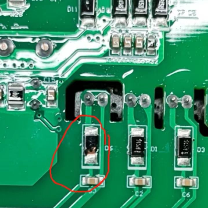
The excessive area of soldering tin has an impact on electronic components
In PCBA (Printed Circuit Board Assembly) manufacturing, the control of solder area is crucial as it directly impacts the quality and reliability of the soldering process. Exceeding 100% solder coverage, indicating an excessive amount of solder, can lead to various issues such as asymmetrical solder distribution, internal voids within solder joints, and excess solder, all of which can compromise the electrical performance and longevity of the assembly.
Adverse Effects of Excessive Solder Coverage:
2. Internal Voids in Solder Joints: These voids reduce the mechanical strength and electrical conductivity of the joint, potentially leading to open circuits over time.
3. Excess Solder: Beyond the necessary coverage, excess solder can compromise the aesthetics of the joint and may form protrusions upon cooling, interfering with component functionality or even causing shorts.
Causes of Excessive Spread of Solder (Crawling) During Component Placement:
1. Solder Alloy Composition: The choice of solder alloy significantly affects its wettability and spread. Eutectic alloys are preferred due to their low melting point and good wettability, but incorrect alloy selection can lead to high rates of defects related to excessive solder spread.
2. **Flux Usage**: Flux removes oxides, reduces surface tension, and enhances wettability. Inappropriate flux composition, activity, or application can result in soldering defects like cold or dry joints, impacting solder spread control and contributing to higher defect rates.
4. Welding Process Parameters: These include temperature, time, and pressure. Improper settings can lead to incomplete melting or poor wettability of the solder alloy, resulting in excessive spread. Adjusting these parameters based on alloy properties, surface characteristics, and equipment capabilities is essential to avoid this issue, which tends to have high defect rates.
5. Environmental Factors: Mechanical vibrations, temperature fluctuations, humidity, and corrosive gases can all impact the reliability of solder joints over time, potentially causing cracks or failures that indirectly affect solder spread control. These factors often manifest as fewer defects or occasional failures.
Comprehensive Approach to Control Solder Spread:
To ensure stable soldering quality, it is imperative to consider and adjust the following aspects comprehensively: selecting the appropriate solder alloy, optimizing flux usage, ensuring proper surface preparation, fine-tuning welding process parameters, and mitigating adverse environmental impacts. This holistic approach ensures that the PCBA electronic components are reliably and effectively soldered, enhancing the overall quality and longevity of the product.
https://www.sh-jieenlu.com/